Flash-based SSD Basics
Introduction
In this post, we highlight the key points from Chapter 44: Flash-based SSDs from OSTEP.
Solid-state storage device (SSD) is built out of transistors (like memory and processors) but it can retain information without power. First, we introduce the physical properties of the raw flash. Then, we focus on building a persistent storage device (i.e. NAND-based flash-based SSD)based on those physical properties.
Please note that I organize the post based on my own understanding of the chapter: the organization may not reflect the actual organization of the chapter. I also add a few illustrations to reflect the concepts in the chapter. Black & white pictures are taken from the book while the color ones are the drawings on my own.
Raw Flash
In this section, we introduce the raw flash using the bottom-up approach by first introducing the basic building block: transistor (i.e. cell). Then, we organize those cells into flash planes, which consist of physical blocks and pages. Finally, we introduce the basic operations supported by the raw flash and possible performance and reliability considerations when we build a persistent storage device.
Storing a Single Bit
- Single-level cell (SLC) flash: a transistor (cell) stores a single bit (1 or 0)
- Multi-level cell (MLC) flash: a transistor (cell) stores two bits (00, 01, 10,11)
- Triple-level cell (TLC) flash: a transistor (cell) encodes 3 bits.
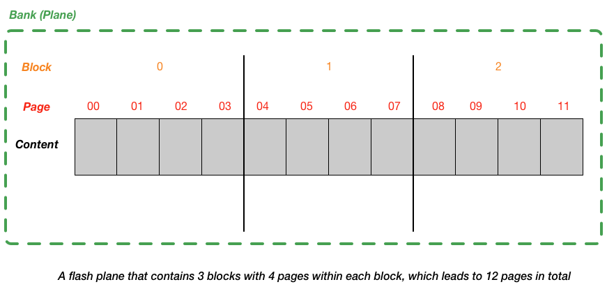
From Bits to Banks/Planes
- Flash chips are organized into banks or planes, which consists of a large number of cells.
-
A bank (plane) is accessed in two different sized units:
- blocks (erase blocks): 128KB or 256KB
- pages: 4KB
Basic Flash Operations
-
Three low-level flash chip operations:
-
Read (a page):
- read any page by specifying page number
- random access device: being able to access any location uniformly quickly (regardless of location on the device and the location of previous request)
-
Erase (a block):
- Before writing to a page within a flash, the device needs to first erase the entire block the page within
- Need to make sure we save the contents of the to-be-erased blocks before executing the erase
- The entire block is reset and each page within is read to be programmed
-
Program (a page):
- Modified the page and write the modification to flash
-
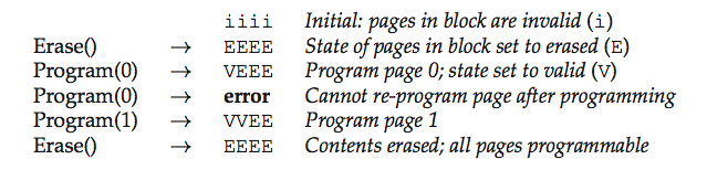
Note
We use \(\texttt{INVALID}\), \(\texttt{ERASED}\), and \(\texttt{VALID}\) to represents three states of a page. One should note that write to a page with state \(\texttt{E}\) doesn’t cause the entire block to be erased. However, to write to a page with state \(\texttt{V}\), the device requires the whole block to be erased.
Flash Performance and Reliability
-
wear out: when a flash block is erased and programmed, it slowly accures a little bit of extra charge. Over time, as that extra charge builds up, it becomes increasingly diffcult to differentiate between a 0 and a 1. At the point where it becomes impossible, the block becomes unusable.
-
disturbance: when accessing a particular page within a flash, it is possible that some bits get flipped in neighboring pages; such bit flips are known as read disturbs or program disturbs, depending on whether the page is being read or programmed, respectively.
From Raw Flash to Flash-Based SSDs
- Goal: standard storage interface is bocked-based one, where blocks (sectors) of size 512 bytes can be read or written, given a block address. Thus, flash-based SSD is to provide that standard block interface atop the raw flash chips inside it.
The organization of Flash-based SSD
-
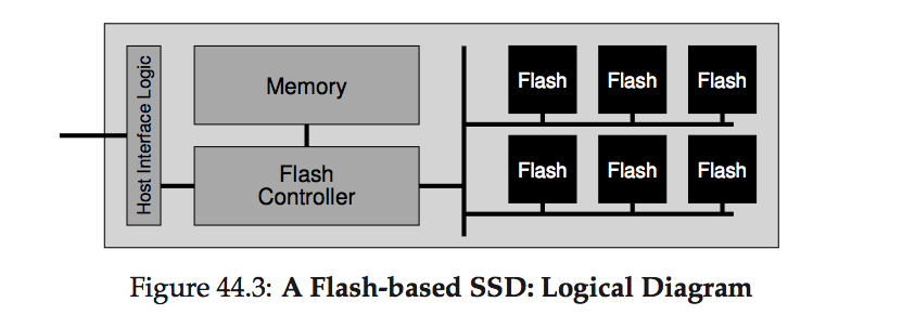
SSD consists of:
- Flash chips: for persistent storage
- Volatile memory (SRAM): caching, buffering data, mapping tables
- Control logic (FTL)
Build Flash Translation Layer (FTL)
-
Flash Translation Layer (FTL):
- Translate client reads & writes on logical blocks -> flash read, erase, program on physical blocks & pages
- performance:
- Use multiple flash chips in parallel
- Reduce write amplification: the total write traffic (in bytes) issued to the flash chips by the FTL divided by the total write traffic (in bytes) issued by the client to the SSD.
- reliability:
- wear leveling (prevent wear out): spread writes across the blocks of the flash as evenly as possible, ensuring that all of the blocks of the device wear out at roughly the same time;
- Prevent disturbance: program pages within an erased block in order, from low page to high page
-
Direct-mapped FTL:
- 1-1 mapping between logic page and physical page
- Read of a logical page \(N\) mapped to read of a physical page \(N\) directly
- Overwrtie of a logical page \(N\) leads to the write amplification:
- Read in the entire block that contains physical page \(N\)
- Erase the block
- Program the page \(N\) along with the old pages within the block
- Can lead to wear out if the user repeated update the same logical page (e.g., update the same file system metadata over and over)
- 1-1 mapping between logic page and physical page
-
Log-structured FTL:
-
Upon a write to a logical block \(N\), the device appends the write to the the next free spot in the currently-being-written-to block.
-
Write: the SSD finds a location for the write, usually just picking the next free page; it then programs that page with the block’s contents, and records the logical-to-physical mapping in its mapping table.
-
Read: subsequent reads use the table to translate the logical block address presented by the client into the physical page number required to read the data.
-
Advantages:
- We avoid the overwrite of the physical page (by always writing to the next free page), which can cause the expensive erase operation and write amplification.
- FTL spreads the write across all pages and perform wear leveling to increase the lifetime of the device.
-
Disadvantages:
- Need to periodically perform garbage collection, which can increase write amplification and reduce performance
- High cost of in-memory mapping tables (the larger the device, the more memory such tables need)
-
crash recovery:
- Since mapping table is stored in memory, we may lose it when device loses power. To handle this, we can store some mapping information in out-of-band (OOB) area within each page and reconstruct the mapping table in memory.
- Use logging and checking to speed up recovery.
-
-
Garbage Collection (dead-block reclamation):
- Garbage: old versions of data around the drive that takes up the space
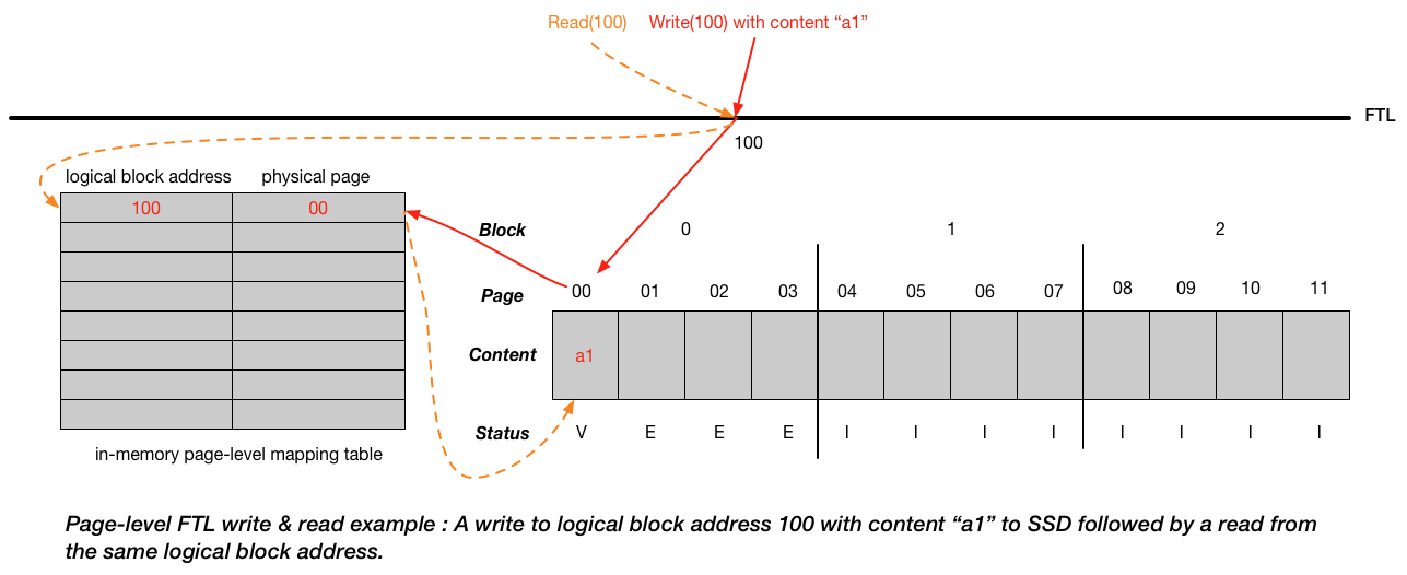
- Ex: immediately follow the picture above, we write(100) with content “c1”. The original “a1” is no longer needed, which is considered as garbage. We need to reclaim the physical page that “a1” takes.
- Garbage collection: the process of finding garbage blocks and reclaiming them for future use. We can find a block that contains one or more garbage pages, read in the live (non-garbage) pages from that block, write out those live pages to the log, and (finally) reclaim the entire block for use in writing.
- Determine the dead pages: the physical block contains the logical block addresses it is holding. We can then determine the dead pages by comparing the logical block addresses in the mapping table with the logical block addresses in the physical block (e.g., physical block holds logical block address 2000 but 2000 inside the mapping table pointing to the physical page that is outside of the current physical block. Thus, we know the physical page that holds 2000 inside the physical block is the dead page).
- The ideal candidate for reclamation is a block that consists of only dead pages; in this case, the block can immediately be erased and used for new data, without expensive data migration.
- Reduce GC costs: overprovision the device (adding extra flash capacity)
- Garbage: old versions of data around the drive that takes up the space
-
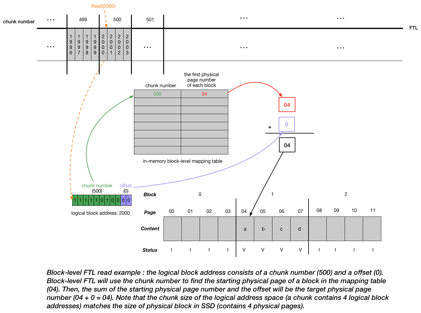
Block-Based Mapping:
- Instead of keeping one record per page in the mapping table, we keep one record per block. Doing so will reduce the size of mapping table by a factor of \(\frac{Size_{block}}{Size_{page}}\).
- Read: The read of a logical block address is shown in picture below. The whole read process greatly mimics the virtual address translation. The mapping table plays a role as the page table in the virtual memory system (map virtual pages to physical frames).
- Write: if the client writes to logical block 2002 with content \(c'\), since by the current mapping, we try to overwrite the physical page with new content, FTL has to perform erase. FTL will read in 2000, 2001, and 2003 and then write out all four logical blocks in a new location (e.g. physical pages 08,09,10,11 with values a, b, c’, d), updating the mapping table accordingly and erase the original block. We can transfer the a,b,c’,d back to the original block but that will involve another set of writes, which are expensive compared with updating the mapping table record.
- Disadvantage: performance decrease for the writes smaller than the physical block size of the device (If the writes equal to the physical block size, we can erase the whole block and do write directly instead of saving some old data and rewrite them again into new location.)
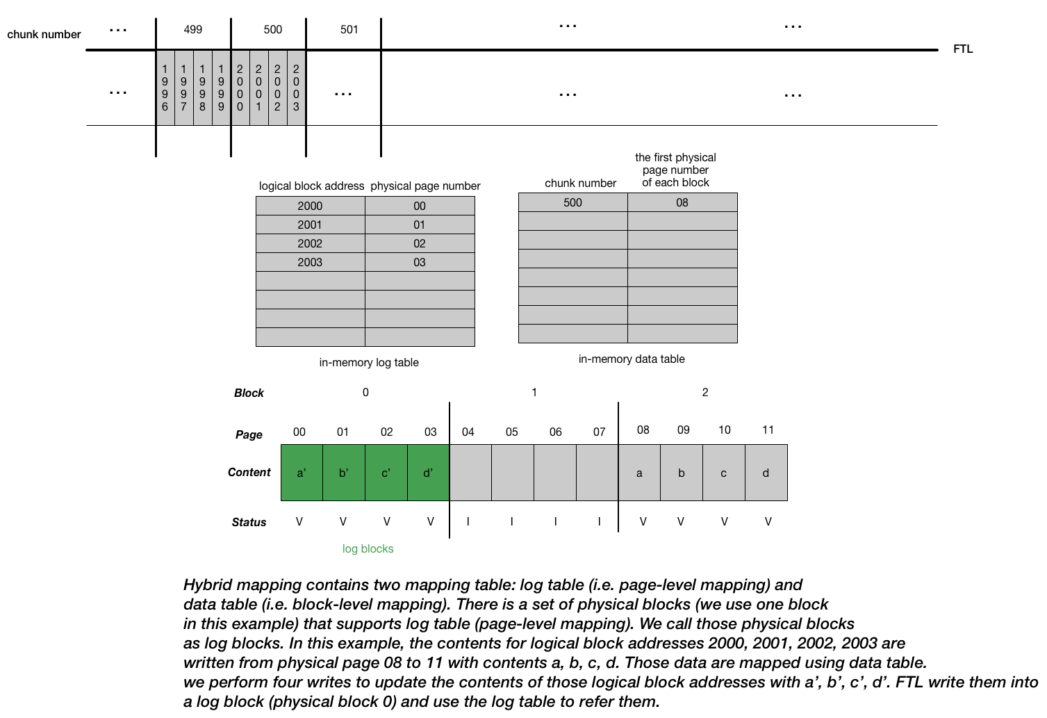
- Hybrid Mapping
- Combine the page-level mapping (enable flexible writing) + block-level mapping (reduce mapping costs)
- FTL structure is shown in the picture below.
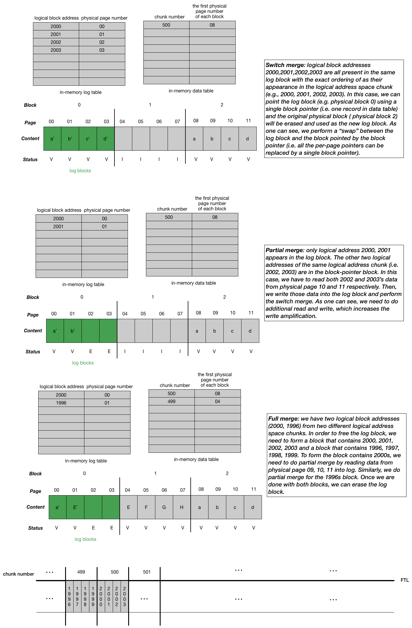
- One big challenge in the hyprid mapping FTL is the “compaction”, which means we have to move the contents from log blocks referred by the log table into the physical blocks referred by the data table. The motivation is that we want to keep the size of log table small (i.e. reduce mapping costs). There are three ways we can perform depends on the contents of the blocks: switch merge, partial merge, full merge shown in the picture below.
Note
“compaction” isn’t a term used in the chapter. I use the term as a way to indicate the whole moving log block process greatly mimics how the compaction works in the Log-structured merge (LSM) tree. Log blocks can be thought of as “memtable” in the LSM-based key-value store. In addition, when we look for a particular logical block, the FTL will first consult the log table; if the logical block’s location is not found there, the FTL will then consult the data table to find its location and then access the requested data. Also, we need to periodically scan the log table and corresponding log blocks to form blocks pointed by only one block pointer. All these behaviors are similar to how read and compaction work in the LSM-based key-value store.
- wear leveling
- Log-structured approach + garbage collection helps with the wear leveling
- Problem: sometimes a block will be filled with long-lived data that does not get overwritten; in this case, garbage collection will never reclaim the block, and thus it does not receive its fair share of the write load.
- Solution: the FTL must periodically read all the live data out of such blocks and re-write it elsewhere, thus making the block available for writing again.
Flash-based SSD performance
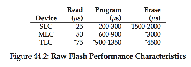
- The biggest difference in performance, as compared to disk drives, is realized when performing random reads and writes.
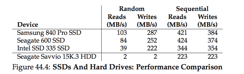
- Findings in the above table:
- SSD random I/O outperforms HDD random I/O
- SSD sequential I/O is slightly above HDD sequential I/O (i.e. HDD still in the game for the sequential I/O task)
- SSD random write beat random read
- log-structured design of many SSDs, which transforms random writes into sequential ones and improves performance.
- HDD is still cheaper than SSD
Summary
-
Overwriting a page requires us to erase the whole block that the page resides in before we can write the page. This naturally introduces the write amplification as we must first move any data we care about to another location.
-
When design a persistent storage device based on flash, we need to think about performance (e.g. write amplification) and reliability (e.g. wear out, disturbance).
-
Log-structured hybrid mapping FTL provides an interface that maps the I/O to logical address space to the physical blocks & pages on the flash chips while maintaining good performance and reliability.